Intel's Billion-Dollar Chipmaking Process Uses Precision Lasers and AI to Etch Patterns Measured in Atoms
-
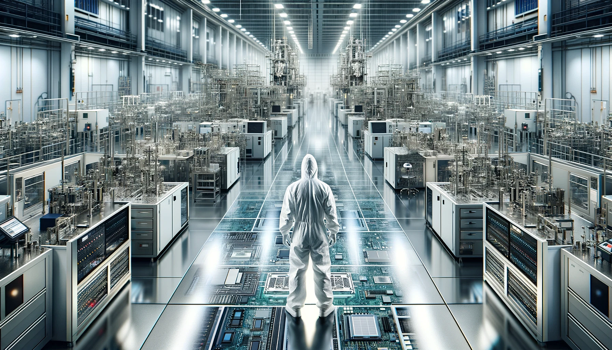
Intel's chip manufacturing is extremely complex, requiring nanometer precision. It's compared to a bakery with very expensive "ovens" that take years and billions to develop.
-
Photolithography machines etch transistor patterns just atoms wide into silicon wafers. Smaller wavelengths enable smaller transistors per Moore's law.
-
EUV lithography uses extreme ultraviolet light, generated by hitting tin droplets with lasers to create plasma. This machine took 17 years and $6 billion to develop.
-
Everything is automated in the manufacturing process. Precise recipes are designed, then chips are manufactured without human intervention.
-
Machine learning helps optimize every step, from computer vision for inspection to natural language processing to parse equipment logs.